- 您现在的位置:买卖IC网 > Sheet目录3887 > PIC16F872T-E/SO (Microchip Technology)IC MCU CMOS 20MHZ 2K FLSH 28SOIC
164
8048C–AVR–02/12
ATtiny43U
20.8
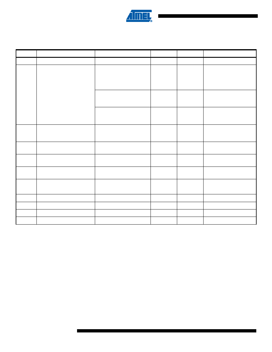
ADC Characteristics
Note:
1. Gain error also depends on the accuracy of the selected reference source. When using VCC as a reference it should be
noted that the output voltage of the boost converter has a wide dynamic range, especially in Active Low Current Mode. The
internal voltage reference is rather immune to variations in supply voltage and is therefore the recommended reference
source to be used. See “Bandgap Voltage vs. Supply Voltage” on page 189.
Table 20-8.
ADC Characteristics, Single-Ended Conversion, T
A = -40°C to +85°C, Boost Converter Enabled.
Symbol
Parameter
Condition
Min
Typ
Max
Units
Resolution
10
Bits
Absolute accuracy (1)
(Including INL, DNL, and
quantization, Gain and Offset
Errors)
V
REF = VCC = 3V
ADC clock = 200 kHz
3.5
LSB
VREF = VCC = 3V
ADC clock = 1 MHz
4.0
LSB
VREF = VCC = 3V
ADC clock = 200 kHz
Noise Reduction Mode
3.0
LSB
VREF = VCC = 3V
ADC clock = 1 MHz
Noise Reduction Mode
3.5
LSB
Integral Non-linearity (INL) (1)
(Accuracy after Offset and
Gain Calibration)
V
REF = VCC = 3V
ADC clock = 200 kHz
1.0
LSB
Differential Non-linearity
(DNL)
VREF = VCC = 3V
ADC clock = 200 kHz
0.5
LSB
Gain Error (1)
V
REF = VCC = 3V
ADC clock = 200 kHz
5.0
LSB
Offset Error
VREF = VCC = 3V
ADC clock = 200 kHz
-3.0
LSB
Conversion Time
Free Running Conversion
14
280
s
Clock Frequency
50
1000
kHz
V
IN
Input Voltage
GND
V
REF
V
Input Bandwidth
38.4
kHz
V
INT
Internal Voltage Reference
1.0
1.1
1.2
V
R
AIN
Analog Input Resistance
100
M
Ω
发布紧急采购,3分钟左右您将得到回复。
相关PDF资料
PIC16F727-E/P
IC PIC MCU FLASH 8KX14 40-DIP
PIC16F871T-E/PT
IC MCU CMOS 20MHZ 2K FLSH 44TQFP
PIC16F871T-E/L
IC MCU CMOS 20MHZ 2K FLSH 44PLCC
PIC16F871-E/PT
IC MCU CMOS 20MHZ 2K FLSH 44TQFP
PIC16F871-E/L
IC MCU CMOS 20MHZ 2K FLSH 44PLCC
PIC16F870T-E/SS
IC MCU CMOS 20MHZ 2K FLSH 28SSOP
PIC16F870T-E/SO
IC MCU CMOS 20MHZ 2K FLSH 28SOIC
PIC16F84AT-20E/SS
IC MCU CMOS 20MHZ 1K FLSH 20SSOP
相关代理商/技术参数
PIC16F872T-E/SS
功能描述:8位微控制器 -MCU 3.5KB 128 RAM 22 I/O RoHS:否 制造商:Silicon Labs 核心:8051 处理器系列:C8051F39x 数据总线宽度:8 bit 最大时钟频率:50 MHz 程序存储器大小:16 KB 数据 RAM 大小:1 KB 片上 ADC:Yes 工作电源电压:1.8 V to 3.6 V 工作温度范围:- 40 C to + 105 C 封装 / 箱体:QFN-20 安装风格:SMD/SMT
PIC16F872T-I/SO
功能描述:8位微控制器 -MCU 3.5KB 128 RAM 22 I/O RoHS:否 制造商:Silicon Labs 核心:8051 处理器系列:C8051F39x 数据总线宽度:8 bit 最大时钟频率:50 MHz 程序存储器大小:16 KB 数据 RAM 大小:1 KB 片上 ADC:Yes 工作电源电压:1.8 V to 3.6 V 工作温度范围:- 40 C to + 105 C 封装 / 箱体:QFN-20 安装风格:SMD/SMT
PIC16F872T-I/SS
功能描述:8位微控制器 -MCU 3.5KB 128 RAM 22 I/O RoHS:否 制造商:Silicon Labs 核心:8051 处理器系列:C8051F39x 数据总线宽度:8 bit 最大时钟频率:50 MHz 程序存储器大小:16 KB 数据 RAM 大小:1 KB 片上 ADC:Yes 工作电源电压:1.8 V to 3.6 V 工作温度范围:- 40 C to + 105 C 封装 / 箱体:QFN-20 安装风格:SMD/SMT
PIC16F872T-I/SS033
制造商:Microchip Technology Inc 功能描述:
PIC16F873-04/SO
功能描述:8位微控制器 -MCU 7KB 192 RAM 22 I/O RoHS:否 制造商:Silicon Labs 核心:8051 处理器系列:C8051F39x 数据总线宽度:8 bit 最大时钟频率:50 MHz 程序存储器大小:16 KB 数据 RAM 大小:1 KB 片上 ADC:Yes 工作电源电压:1.8 V to 3.6 V 工作温度范围:- 40 C to + 105 C 封装 / 箱体:QFN-20 安装风格:SMD/SMT
PIC16F873-04/SO
制造商:Microchip Technology Inc 功能描述:8BIT FLASH MCU SMD 16F873 SOIC28
PIC16F873-04/SP
功能描述:8位微控制器 -MCU 7KB 192 RAM 22 I/O RoHS:否 制造商:Silicon Labs 核心:8051 处理器系列:C8051F39x 数据总线宽度:8 bit 最大时钟频率:50 MHz 程序存储器大小:16 KB 数据 RAM 大小:1 KB 片上 ADC:Yes 工作电源电压:1.8 V to 3.6 V 工作温度范围:- 40 C to + 105 C 封装 / 箱体:QFN-20 安装风格:SMD/SMT
PIC16F873-04/SP
制造商:Microchip Technology Inc 功能描述:IC 8BIT FLASH MCU 16F873 SDIL28